A quick peek into the report
Metalens Market Overview
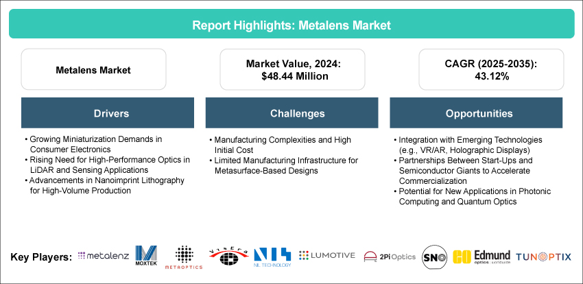
The metalens market was valued at approximately $48.44 million in 2024 and is projected to grow at a CAGR of 43.12%, reaching $3,561.84 million by 2035. Growth in the metalens market has been driven by increasing demand for compact, high-performance optical components across applications such as consumer electronics, AR/VR devices, automotive sensing, healthcare imaging, aerospace and defense, and optical communications. Metalenses enable reductions in size, weight, and optical complexity, positioning the metalens market as a disruptive alternative to conventional refractive and diffractive optics. Adoption within the metalens market is supported by the growing integration of advanced sensing and imaging functions in smartphones, depth-sensing modules, LiDAR systems, and near-eye displays. As device manufacturers pursue thinner form factors and higher functional density, the metalens market benefits from the ability of metalenses to simplify optical stacks while maintaining or improving performance. Advances in nanoimprint lithography (NIL), wafer-level manufacturing, and CMOS-compatible fabrication processes are expected to enhance yield and cost efficiency, supporting broader adoption across the metalens market. While near-term adoption in the metalens market remains concentrated in high-value and performance-critical applications, continued progress in manufacturing and system integration is expected to expand addressable opportunities over the forecast period.
Introduction of Metalens
The study conducted by BIS Research highlights the metalens market as a significant advancement in optical system design, enabling planar, nanoscale alternatives to conventional refractive and diffractive lenses. Metalenses provide enhanced control over light propagation while supporting a wide range of optical functions, including focusing, beam shaping, polarization control, and wavelength selectivity. These capabilities contribute to reductions in size, weight, and optical stack complexity across imaging and sensing systems. The planar architecture of metalenses allows for more efficient optical integration, enabling the incorporation of advanced features such as compact camera modules, depth-sensing systems, and near-eye display optics. By improving optical efficiency and simplifying system design, metalenses offer an effective and scalable solution for manufacturers seeking high-performance optics without the bulk and alignment complexity of traditional lens assemblies. This positions the metalens market as a key enabling technology across modern optical platforms, enhancing functionality while supporting miniaturization and system integration. As industries continue to demand higher performance within constrained form factors, the adoption of metalenses is expected to play a critical role in enabling next-generation imaging, sensing, and display solutions. With their ability to deliver multifunctionality in a single optical element, metalenses are positioned to drive the next phase of innovation in optical engineering.
Market Introduction
The global metalens market has been experiencing notable growth as multiple industries increasingly focus on miniaturization, optical integration, and advanced sensing capabilities. Metalenses, which offer planar and nanoscale alternatives to conventional refractive optics, are becoming essential in supporting the integration of compact optical components across applications such as imaging, sensing, and display systems. As manufacturers aim to enhance optical performance, reduce system complexity, and enable thinner form factors, demand in the metalens market is expected to rise steadily. Additionally, metalenses facilitate the integration of advanced optical functionalities such as depth sensing, beam shaping, and near-eye display optics, further driving their adoption. The metalens market is particularly positioned for expansion as device and system developers seek scalable and cost-efficient solutions to meet performance requirements without increasing size, weight, or alignment complexity. This growth is supported by advances in nanofabrication techniques, increasing adoption of wafer-level optics, and growing interest from semiconductor and photonics ecosystems. Furthermore, regions such as Asia-Pacific, North America, and Europe are leading adoption, with Asia-Pacific demonstrating strong momentum due to its dominance in semiconductor manufacturing and consumer electronics production. As optical systems continue to evolve toward higher functional density, the metalens market is expected to play a pivotal role in shaping next-generation optical architectures, offering a balance of performance, integration efficiency, and long-term scalability.
Industrial Impact
The adoption of metalenses is having a meaningful impact across multiple industries, reshaping optical system design and accelerating the shift toward miniaturized, integrated, and high-performance optics. Metalenses enable system developers to replace bulky, multi-element lens assemblies with planar optical components, improving optical efficiency while reducing size, weight, and alignment complexity. By supporting advanced functionalities such as beam shaping, polarization control, depth sensing, and wavelength-specific imaging, metalenses help manufacturers meet growing performance requirements across imaging, sensing, and display applications.
The industrial impact of the metalens market extends beyond end-product manufacturers to a broader ecosystem that includes semiconductor fabs, nanofabrication tool providers, optical materials suppliers, and photonics integrators. Progress in fabrication approaches such as nanoimprint lithography and wafer-level processing is creating new opportunities for collaboration between optics specialists and semiconductor manufacturing players. As demand for compact optical modules increases in applications such as consumer electronics, AR/VR, automotive sensing, healthcare imaging, and aerospace and defense, metalenses are becoming a key enabling technology within next-generation optical architectures.
As industries continue to pursue higher functional density and system integration, the metalens market is expected to drive sustained innovation across the optical value chain, supporting new product designs and long-term shifts in how optical systems are engineered and manufactured.
Market Segmentation:
Segmentation 1: by End-Use Application
• Consumer Electronics
• Healthcare and Medical Imaging
• Automotive and LiDAR
• Aerospace and Defense
• Optical Communications
• Security and Surveillance
• Others
Consumer Electronics to Lead the Metalens Market (by End-Use Application)
Consumer electronics represented the largest end-use segment in the metalens market in 2024, accounting for the highest share of market value among all applications. Leadership of this segment is driven by the growing integration of metalenses into smartphones, depth-sensing modules, camera systems, and emerging AR/VR devices, where compact form factors and high optical performance are critical. Consumer electronics manufacturers increasingly evaluate metalenses to reduce optical stack thickness, simplify multi-lens assemblies, and enable advanced imaging and sensing functionalities within constrained device designs.
The dominance of consumer electronics reflects the sector’s ability to absorb early adoption of new optical technologies at scale, supported by large production volumes and rapid product cycles. As device makers continue to prioritize miniaturization, improved imaging capabilities, and integration of advanced sensing features, consumer electronics are expected to remain the primary driver of metalens deployment. This positioning establishes consumer electronics as the leading application segment in the metalens market, setting the foundation for broader adoption across other end-use industries over time.
Segmentation 2: by Wavelength
• Ultraviolet (UV)
• Visible
• Near-Infrared (NIR)
• Infrared (IR)
Near-Infrared (NIR) to Lead the Metalens Market (by Wavelength)
The near-infrared (NIR) wavelength segment represented the largest share of the metalens market by value in 2024, making it the leading wavelength category among ultraviolet, visible, and infrared bands. NIR metalenses are widely deployed in applications such as depth sensing, 3D imaging, LiDAR, biometric sensing, and machine vision, where NIR wavelengths offer advantages in penetration, signal stability, and compatibility with existing sensor architectures.
The dominance of the NIR segment reflects its strong alignment with high-volume and high-growth applications, particularly in consumer electronics, automotive sensing, and industrial and security imaging. NIR wavelengths are commonly used in structured light and time-of-flight systems, driving early and sustained adoption of metalenses optimized for this spectral range. As a result, NIR metalenses account for the highest market value within the overall wavelength segmentation, positioning the segment as the primary contributor to revenue in the metalens market.
Segmentation 3: by Fabrication Method
• Nanoimprint Lithography (NIL)
• Electron Beam Lithography (EBL)
• Laser Interference Lithography
• Others (Focused Ion Beam, UV Lithography, etc.)
Nanoimprint Lithography (NIL) to Lead the Metalens Market (by Fabrication Method)
Nanoimprint lithography (NIL) showcased the leading fabrication method in the metalens market by value in 2024, accounting for the largest share among all manufacturing approaches. NIL’s leadership is driven by its ability to support wafer-scale replication, high throughput, and lower per-unit cost compared with serial techniques such as electron beam lithography. These characteristics make NIL the most commercially viable pathway for scaling metalens production beyond research and pilot volumes.
The dominance of NIL reflects its growing adoption in consumer electronics, near-infrared sensing, and automotive and industrial imaging applications, where volume production and cost efficiency are critical. As metalenses transition from laboratory-scale demonstrations toward broader commercialization, NIL has emerged as the preferred fabrication method for enabling repeatable manufacturing while maintaining nanoscale pattern fidelity. As a result, NIL accounts for the highest market value within the fabrication-method segmentation, positioning it as the primary enabler of large-scale metalens adoption.
Segmentation 4: by Region
• North America: U.S. and Canada
• Europe: Germany, France, U.K., Italy, Netherlands, and Rest-of-Europe
• Asia-Pacific: China, Japan, South Korea, Australia, and Rest-of-Asia-Pacific
• Rest-of-the-World
Europe represents the leading regional market for metalenses by value in 2024, accounting for the highest share among all regions. The region’s leadership is driven by its strong base in advanced photonics research, precision optics manufacturing, and early commercial adoption of metalenses across high-value applications. European demand is concentrated in automotive and LiDAR systems, industrial and scientific imaging, aerospace and defense optics, and optical instrumentation, where performance, reliability, and system qualification are critical.
Europe’s position is reinforced by sustained public funding and coordinated research–industry collaboration, which supports the transition of metalenses from laboratory development to pilot and early commercial deployment. The region hosts a dense ecosystem of photonics institutes, optics manufacturers, and system integrators that actively evaluate metalenses for compact sensing, imaging, and wavelength-specific applications. As a result, Europe captures the largest market value in the metalens market in 2024, reflecting its role as a validation- and application-driven adoption hub.
While Asia-Pacific demonstrates strong growth potential due to manufacturing scale and consumer electronics demand, Europe’s early adoption in high-value and performance-critical applications positions it as the leading regional contributor to market value at this stage. This establishes Europe as the primary regional market for metalenses in the current market landscape.
Demand - Drivers, Limitations, and Opportunities
Market Demand Drivers: Rising Demand for Optical Miniaturization and Performance Efficiency
The demand for advanced optical miniaturization is a key driver in the metalens market, as industries across consumer electronics, sensing, and imaging push for higher functionality within increasingly constrained form factors. Device manufacturers face growing pressure to integrate high-performance cameras, depth sensors, and optical modules without increasing size, weight, or system complexity. Traditional multi-element refractive optics often limit further miniaturization due to thickness, alignment requirements, and assembly constraints, creating a structural shift toward planar metasurface-based alternatives.
Metalenses enable precise wavefront control in a single flat element, supporting compact optical architectures that align with next-generation product design priorities. Adoption is particularly strong in consumer electronics, near-infrared sensing, biometric authentication, and AR/VR devices, where form-factor reduction and optical efficiency directly influence product differentiation. As optical systems increasingly converge with semiconductor-based platforms, the metalens market benefits from its compatibility with wafer-level manufacturing and CMOS integration.
Market Challenges: Manufacturing Scalability and Integration Complexity
Despite strong demand drivers, the metalens market faces challenges related to manufacturing scalability, yield consistency, and system integration. Metalenses require nanostructures with subwavelength precision, making fabrication more complex than conventional lens manufacturing. Variations in feature geometry or etch depth can significantly impact optical performance, necessitating tight process control and advanced metrology.
In addition, integrating metalenses into existing optical modules often requires redesign of packaging, alignment, and testing workflows that have been optimized for curved optics. The absence of universally adopted standards for meta-optic qualification further slows adoption in regulated or high-reliability applications such as automotive sensing, medical imaging, and aerospace systems. Overcoming these manufacturing and integration barriers remains essential for the broader commercialization of metalenses beyond early pilot deployments.
Market Opportunities: Expansion across High-Volume and High-Value Optical Applications
The metalens market presents substantial opportunities across both high-volume and high-value application segments. In consumer electronics, metalenses enable thinner camera modules, advanced facial recognition systems, and compact depth-sensing solutions. In AR/VR and spatial computing, metasurfaces support near-eye optics, eye-tracking modules, and beam-shaping components that are critical for lightweight and ergonomic device designs.
Additional opportunities are emerging in automotive LiDAR, industrial vision, healthcare imaging, security and surveillance, and optical communications, where performance-driven demand can support early-stage manufacturing costs. Continued progress in nanoimprint lithography, wafer-level optics, and semiconductor-aligned fabrication is expected to improve cost efficiency over time, enabling metalenses to penetrate more cost-sensitive applications. As integration pathways mature, metalenses are positioned to transition from niche adoption to broader deployment across the optical value chain.
Analyst View
According to Dhrubajyoti Narayan, Principal Analyst at BIS Research, “the metalens market is positioned for sustained growth as optical systems across multiple industries undergo a structural transition toward miniaturized, integrated, and multifunctional architectures. Demand is being shaped less by direct replacement of conventional lenses and more by the need for form-factor reduction, wavelength-specific performance, and system-level integration.”
He further notes that “consumer electronics currently anchor adoption due to scale and rapid product cycles, while applications such as automotive sensing, AR/VR, and defense imaging provide important validation pathways. Manufacturing execution, particularly the ability to scale nanoimprint lithography with high yield, will be the critical determinant of long-term market expansion. As fabrication and integration challenges are progressively addressed, metalenses are expected to become a foundational component in next-generation optical systems.”
Metalens Market - A Global and Regional Analysis
Focus on Application, Product, and Regional Analysis - Analysis and Forecast, 2025-2035
Frequently Asked Questions
Metalenses are advanced flat optical components based on metasurfaces composed of nanoscale structures that precisely control the phase, amplitude, and polarization of light. Unlike traditional curved lenses, metalenses are ultra-thin and can perform multiple optical functions within a single planar layer. They are used in applications such as imaging, depth sensing, LiDAR, AR/VR systems, biomedical imaging, and optical communications. Metalenses enable reductions in size, weight, and optical complexity while supporting high-performance light manipulation across different wavelengths.
Key business opportunities in the metalens market arise from growing demand for compact, high-performance optics across consumer electronics, AR/VR devices, automotive sensing, healthcare imaging, aerospace and defense, and security applications. Manufacturers can capitalize on these opportunities by developing scalable metalens designs optimized for near-infrared and visible wavelengths, improving wafer-level fabrication techniques, and enabling integration with CMOS sensors. Asia-Pacific presents significant opportunities due to its dominance in semiconductor manufacturing and consumer electronics production, while Europe and North America offer strong demand in high-value and performance-critical applications.
To strengthen their position in the metalens market, existing players are adopting several strategic initiatives:
• Strategic Partnerships and Collaborations: Alliances with semiconductor foundries, optics suppliers, and system integrators to accelerate commercialization and scale production.
• Investment in Research and Development: Focus on improving metasurface design, broadband performance, and fabrication yield through advanced nanofabrication techniques.
• Geographical Expansion: Establishing manufacturing and partnership presence in regions with strong photonics and semiconductor ecosystems.
• Product Development: Launching application-specific metalenses for sensing, imaging, and near-eye display systems.
• Mergers and Acquisitions: Acquiring complementary design capabilities, fabrication expertise, or access to established customer networks.
A new entrant in the metalens market should focus on differentiated metasurface design, scalable fabrication strategies, and application-driven solutions. Priorities include developing metalenses optimized for high-volume applications such as consumer electronics and sensing, establishing early partnerships with semiconductor foundries or optical module manufacturers, and addressing integration challenges related to packaging and testing. Emphasizing manufacturability, cost efficiency, and compatibility with existing optical and semiconductor workflows will be critical for long-term competitiveness.
The USP of this report lies in its comprehensive and structured analysis of the metalens market, covering end-use applications, wavelength segmentation, fabrication methods, and regional dynamics. It provides in-depth insights into market drivers, challenges, and opportunities, supported by technology assessments, competitive benchmarking, and real-world adoption examples. The report also highlights manufacturing scalability, ecosystem partnerships, and emerging application areas, enabling stakeholders to make informed strategic and investment decisions in a rapidly evolving optical technology landscape.
This report is intended for metalens and metasurface technology providers, optical component manufacturers, semiconductor companies, system integrators, and OEMs seeking to understand market opportunities and adoption trends. Investors and venture capital firms evaluating emerging photonics technologies will find valuable insights into growth potential and competitive dynamics. In addition, research institutions, government agencies, and consulting organizations involved in advanced optics, imaging, and sensing technologies can leverage the report to support strategic planning and policy development.